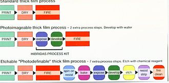
Photoimageable thick-film technology
This article may be too technical for most readers to understand. (December 2011) |

Photoimageable thick-film technology<ref>Hibridas Enterprise</ref> is a combination of conventional thick film technology with elements of thin film technology, and it provides a low cost solution to producing high quality microwave circuits. The ability to directly photoimage the printed layers means that the technology can provide the high line and gap resolution required by high frequency planar components.<ref>D. Stephens, P. R. Young, and I. D. Robertson, "Design and characterization of 180GHz filters in photoimageable thick-film technology", IEEE MTT-S Int. Microwave Symp. Dig., 2005, pp. 451–454.</ref><ref>C. Y. Ng, M. Chongcheawchamnan, M. S. Aftanasar, I. D. Robertson, and J. Minalgience, "X-band microstrip bandpass filter using photoimageable thick-film materials", IEEE MTT-S Int. Microwave Symp. Dig., Vol. 3, 2002, pp. 2209–2212.</ref> It provides a feasible fabrication process to produce circuits operating at microwave and millimetre-wave frequencies. Circuits made using this technology meet the modern requirements for high density packaging, whilst yielding the high quality components required for very high frequency applications, including wireless communication, radar and measurement systems.
This technology also enables both single-layer and multi-layer filters to be produced conveniently. Recent research work<ref>R.A. Tacken, D. Mitcan, and J. Nab, "Combining fine line photoimageable with multi-layer thick film for improved circuit density", CICMT Proceedings, 2017.</ref> has investigated the combination of conventional thick film and fine line photoimageable technologies, in order to accommodate fine pitch and high density applications on the ceramic substrates. Furthermore, previous work<ref>C.-M. Tsai, and K. C. Gupta, "A generalized model for coupled lines and its applications to two-layer planar circuits", IEEE Transactions on Microwave Theory & Techniques, Vol. 40, No. 12, 1992.</ref> has shown that this technology is capable of realizing the circuit quality necessary for high performance microwave components.
Benefits of choosing this structure

Edge coupled band-pass filters were chosen for this study as they are one of the most common and useful microwave and millimetre-wave planar components. The filter performance is based on the coupling between the resonant sections and controlled by the size of the gap.<ref>[2] T. C. Edwards, and M. B. Steer, Foundation of Interconnect and Microstrip Design, J. Wiley & Sons, 2000.</ref> This characteristic makes edge coupled band-pass filters very sensitive to fabrication errors.
Another reason of choosing this structure in a multi-layer form is due to limitation on the structure when it has been fabricated on a single layer. The gap between the two resonant structures becomes very small and cannot easily be fabricated due to the limitations of low-cost fabrication technologies. In multi-layer circuits, the coupling between resonant sections is achieved by overlapping conductors which are separated by a thin dielectric layer. However, to some extent the problem of fabricating small gaps has been exchanged for that of achieving high alignment between the conductor layers. Normally a modern mask aligner will be needed to achieve the required degree of resolution.
Application
The target market for photoimageable thick film pastes is the thick film (hybrid) circuit and component industries plus LTCC and HTCC activities. The technology allows extremely fine lines and structures to be produced with minimal investment in a simple process and use of special paste materials. Most of the production steps needed are already used by the industry. Only two extra production steps are required. No extra clean room requirements are needed. No special lighting is required. No chemicals are required. This can be advantageous for sections of the thick film circuits community which would allow them to offer greater added value, fine line products to compete with other thick film, thin film and PCB technologies.
- High Density Interconnect
- 15 μm line/20 μm space with high yield on alumina ceramic substrates.
- 30 μm line/40 μm space with 50 μm vias for multilayers.
- 20 μm lines/30 μm space within LTCC & HTCC structures.
- RF and microwave (up to 200 GHz is reported)
- Sensor elements (narrow conductors and windows in dielectric and MEMS with ceramic/dielectrics). 10 μm lines/15 μm spaces at 10 μm fired thickness are possible.
- Components, such as fuses & inductors
- Plasma displays and RF shielding on glass
Thick films for microwave applications
Advantages of 'conventional' thick film over thin film
- Through hole metallisation easy for small holes
- A range of resistors is possible
- Low cost process technology
- Added advantages of photoimageable thick film
- Very fine lines with precise geometry, sharp edges
- Low resistivity of fine lines
References
External links
- Aurel Fine Line Equipment, Manufacturer